Multi-Cycle Data path and Control
Last Updated :
01 Oct, 2021
Overview :
Multi-cycle data path break up instructions into separate steps. It reduces average instruction time. Each step takes a single clock cycle Each functional unit can be used more than once in an instruction, as long as it is used in different clock cycles. It reduces the amount of hardware needed.
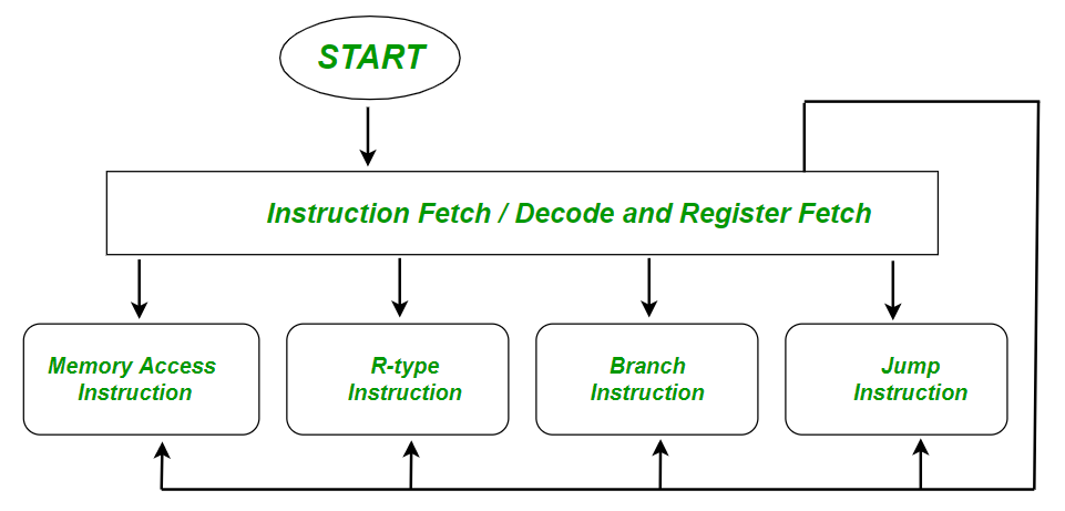
(I) Fetch Instruction :
An instruction stored in the memory is fetched into the control unit of CPU by supplying the memory with the address of the respective given instruction.
- Suppose each instruction is stored in a word and each word is of 4 bytes so we can state that memory is byte addressable here.
- We know, Program Counter (PC) contains the address of next upcoming instruction.
IR <= [[PC]] , PC <= [PC] + 4
(II) Decode (Interpret Instruction) :
The control unit of the processor decodes the instructions in order to find the sequence of operations required to execute the respective instructions.
- Reading of the opcode to determine the type of instructions and field length.
- Then, read in data from all necessary registers.
Example:
A <= Reg [IR [25:21]]; // Register rs in opcode (instruction part)
B <= Reg [IR [25:21]]; // Register rt in opcode (instruction part)
(III) Execution, Memory Address Computation or Branch Instruction :
Examples :
Memory Reference : ALUout   <=   A + sign-extend ( IR[15:0] )
Branch : if (A == B)   PC  <=  ALUout     // Conditional , it will calculate PC= Register + Branch Address
Jump :  PC  <=  PC [ 31:28 ] . ( IR [25 : 0] << 2 )    //// unconditional
(IV) Memory Access / R-type Instruction Completion Step :
Examples :
Memory Reference:  MDR  <=  Memory [ALUout ];    // LOAD  or  Memory [ALUout ]  <=  B;    // Store from register to memory
Arithmetic Logic Instruction (R-type) :  Reg [ IR[15:11]]  <=  ALUout ;      // register destination in opcode
(V) Memory Read Completion Step (Register Write) :
- Most Instruction write the result of some computation into a register.
- Example : Arithmetic, Logical, Shifts, Loads etc. LOAD : Reg [ IR [20:16]] <= MDR
- Stores, branches, jumps do not write in the register at the end and they remain idle.
Examples :
Q1. Find the stages of data path and control (Execution Sequence) for
ADD R1, R2, R3 ;
it means R3 <– R1 + R2
Solution: Given Instruction – ADD R3, R1, R2;
- Stage 1 : Fetch the instruction and increase the program counter.
- Stage 2 : Decode to determine that it is an ADD instruction and, read registers R1 and R2.
- Stage 3 : Add the respective two values retrieved in Stage 2.
- Stage 4 : Idle ( Nothing to write to memory )
- Stage 5 : Write result of Stage 3 in register R3.
Q2. Find the stages of data path and control (Execution Sequence) for
MOV 30 (R1), R2;
it means [30 + R1] <– R2
Solution: Given Instruction – MOV 30 (R1), R2;
- Stage 1 (Fetch) : Fetch the instruction and increase the program counter.
- Stage 2 (Decode) : Decode to find the respective instruction is MOV and, read registers R1 and R2
- Stage 3 (Execute) : Add 30 to value in the respective register R1.
- Stage 4 (Memory Access) : Write value in register R2 into memory address computed in Stage3.
- Stage 5 (Register Write) : This step is idle ( nothing to write in register )
Like Article
Suggest improvement
Share your thoughts in the comments
Please Login to comment...