Synchronous 3 bit Up/Down counter
Last Updated :
26 May, 2021
Prerequisite : 3 bit down counter.
Overview:
- These types of counters fall under the category of synchronous controller counter.
- Here the mode control input is used to decide whether which sequence will be generated by the counter.
- In this case, mode control input is used to decide whether the counter will perform up counting or down counting.
- Designing of such a counter is the same as designing a synchronous counter but the extra combinational logic for mode control input is required.
Steps to design Synchronous 3 bit Up/Down Counter :
1. Decide the number and type of FF –
- Here we are performing 3 bit or mod-8 Up or Down counting, so 3 Flip Flops are required, which can count up to 23-1 = 7.
- Here T Flip Flop is used.
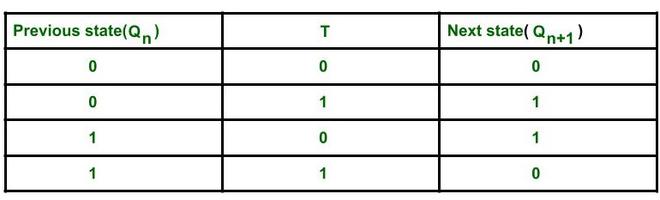
2. Write excitation table of Flip Flop –
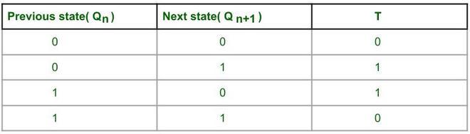
Excitation table of T FF
3. Decision for Mode control input M –
- When M=0 ,then the counter will perform up counting.
- When M=1 ,then the counter will perform down counting.
4. Draw the state transition diagram and circuit excitation table –
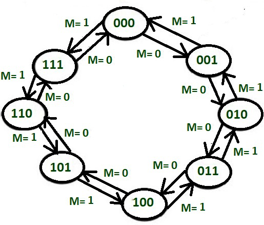
State transition diagram for 3 bit up/down counting.
5. Circuit excitation table –
The circuit excitation table represents the present states of the counting sequence and the next states after the clock pulse is applied and input T of the flip-flops. By seeing the transition between the present state and the next state, we can find the input values of 3 Flip Flops using the Flip Flops excitation table. The table is designed according to the required counting sequence.
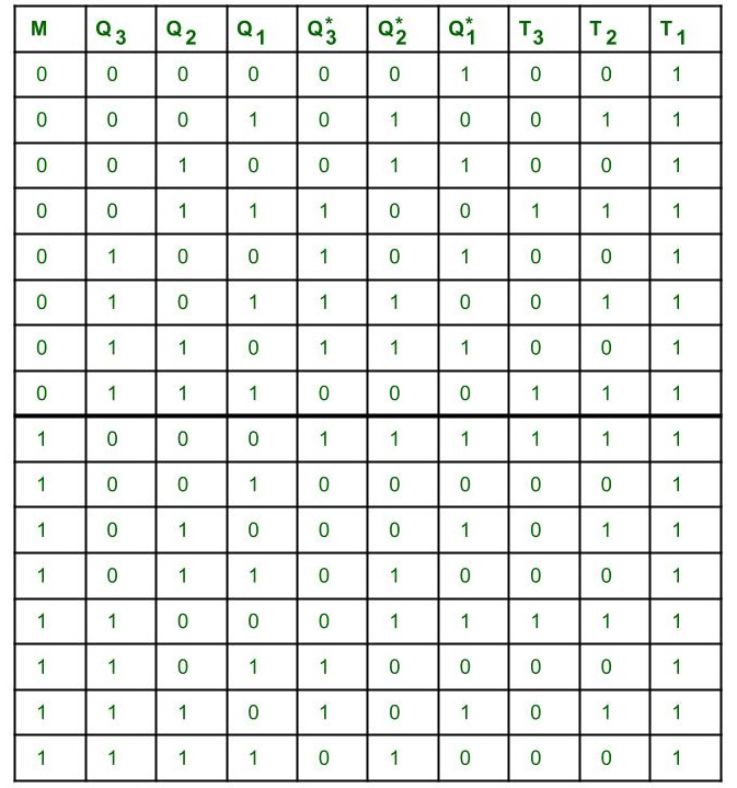
Circuit excitation table
If there is a change in the output state of a flip flop (i.e. 0 to 1 or 1 to 0), then the corresponding T value becomes 1 otherwise 0.
6. Find a simplified equation using k map –
Here we are finding the minimal Boolean expression for each Flip Flop input T using k map.
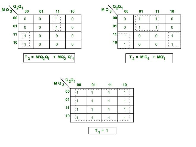
Simplified equation for K map
7. Create a circuit diagram –
The simplified expression for Flip Flops is used to design circuit diagrams. Here all the connections are made according to simplified expressions for Flip Flops.
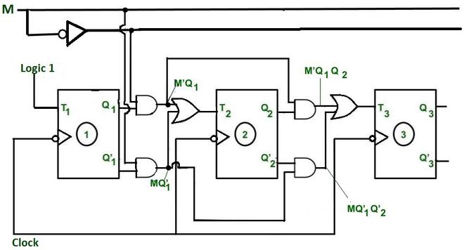
3 bit synchronous up/down counter.
8. Timing Diagram –
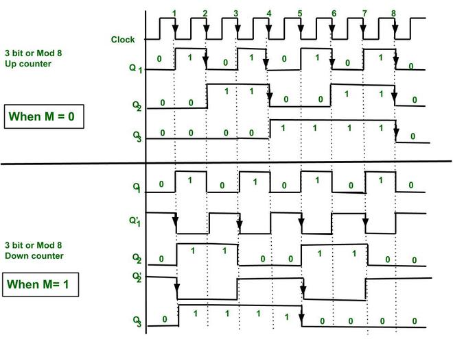
Timing diagram for 3 bit synchronous Up/Down counter
Explanation :
Here -ve edge triggered clock pulse is used for toggling purpose.
Characteristics table of T FF
After every falling edge, when T = 1, the output state of Flip Flop will toggle.
- Initially Q3 = 0 , Q2= 0 , Q1= 0.
Case 1 : When M=0 ,then M’= 1
- T3 = M’Q2Q1 + MQ’2Q’1 = Q2Q1.
- T2 = M’Q1 + MQ’1= 1.Q1= Q1.
- T1= 1.
- Because T1= 1, therefore FF1 output state toggles for every falling edge.
The output state of FF 2 will toggle when Q1 = 1 and the falling edge of the clock pulse occurs.
The output state of FF 3 will toggle only when Q2.Q1= 1 and the falling edge of the clock pulse occurs.
- In this way, after every falling edge, state transition takes place and we can get our desired counting sequence.
Case 2 : When M=1 ,then M’ =0
- T3 = M’Q2Q1+MQ’2Q’1 = Q’2Q’1
- T2 = M’Q1+ MQ’1= 1.Q1= Q’1.
- T1= 1.
- Because T1= 1,therefore FF1 output state toggles for every falling edge.
The output state of FF 2 will toggle when Q’1 = 1 and the falling edge of the clock pulse occurs.
The output state of FF 3 will toggle only when Q’2.Q’1= 1 and the falling edge of the clock pulse occurs.
- In this way, after every falling edge, state transition takes place and we can get our desired counting sequence.
Like Article
Suggest improvement
Share your thoughts in the comments
Please Login to comment...