Timing diagram of INR M
Last Updated :
05 Apr, 2023
Problem – Draw the timing diagram of the given instruction in 8085,
INR M
The content present in the designated register/memory location (M) is incremented by 1 and the result is stored in the same place. If the operand is a memory location, it is specified by the contents of HL pair. Example:
INR M
Opcode: INR
Operand: M
M is the memory location (say 5000H) and suppose the data present at M (or 5000H) is 26H, which is need to be incremented by 1. Hex code- 34H Algorithm – The instruction INR M is of 1 byte; therefore the complete instruction will be stored in a single memory address. For example:
2000: INR M
The opcode fetch will be same as for other instructions in first 4 T states. Only the Memory read and Memory Write need to be added in the successive T states. For the opcode fetch the IO/M (low active) = 0, S1 = 1 and S0 = 1. For the memory read the IO/M (low active) = 0, S1 = 1 and S0 = 0. Also, only 3 T states will be required. For the memory write the IO/M (low active) = 0, S1 = 0 and S0 = 1 and 3 T states will be required. The timing diagram of INR M instruction is shown below: 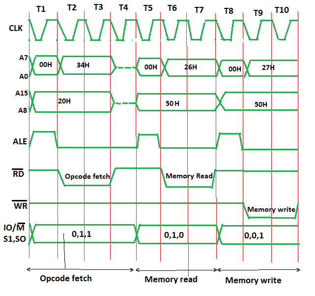 In Opcode fetch ( t1-t4 T states ) –
- 00: lower bit of address where opcode is stored, i.e., 00
- 20: higher bit of address where opcode is stored, i.e., 20.
- ALE: provides signal for multiplexed address and data bus. Only in t1 it used as address bus to fetch lower bit of address otherwise it will be used as data bus.
- RD (low active): signal is 1 in t1 & t4 as no data is read by microprocessor. Signal is 0 in t2 & t3 because here the data is read by microprocessor.
- WR (low active): Signal is 1 throughout, no data is written by microprocessor.
- IO/M (low active): Signal is 0 in throughout because the operation is performing on memory.
- S0 and S1: both are 1 in case of opcode fetching.
In Memory read ( t5-t7 T states ) –
- 00: lower bit of address where opcode is stored, i.e, 00
- 50: higher bit of address where opcode is stored, i.e, 50.
- ALE: provides signal for multiplexed address and data bus. Only in t5 it used as address bus to fetch lower bit of address otherwise it will be used as data bus.
- RD (low active): signal is 1 in t5, no data is read by microprocessor. Signal is 0 in t6 & t7, data is read by microprocessor.
- WR (low active): signal is 1 throughout, no data is written by microprocessor.
- IO/M (low active): signal is 0 in throughout, operation is performing on memory.
- S0 and S1 – S1=1 and S0=0 for Read operation.
In Memory write ( t8-t10 T states ) –
- 00: lower bit of address where opcode is stored, i.e, 00
- 50: higher bit of address where opcode is stored, i.e, 50.
- ALE: provides signal for multiplexed address and data bus. Only in t8 it used as address bus to fetch lower bit of address otherwise it will be used as data bus.
- RD (low active): signal is 1 throughout, no data is read by microprocessor.
- WR (low active): signal is 1 in t8, no data is written by microprocessor. Signal is 0 in t9 & t10, data is written by microprocessor.
- IO/M (low active): signal is 0 in throughout, operation is performing on memory.
- S0 and S1 – S1=0 and S0=1 for write operation.
Advantages of using the timing diagram of INR include:
Better monitoring of anticoagulant therapy: The timing diagram of INR provides healthcare professionals with a better understanding of how well the anticoagulant therapy is working.
Helps to adjust medication dosages: The timing diagram of INR helps healthcare professionals to adjust medication dosages to ensure that the patient is receiving the optimal level of anticoagulation.
Reduces the risk of blood clots and bleeding: The timing diagram of INR helps healthcare professionals to reduce the risk of blood clots and bleeding in patients receiving anticoagulant therapy.
Disadvantages of using the timing diagram of INR include:
Need for frequent blood tests: To create a timing diagram of INR, patients need to undergo frequent blood tests, which can be inconvenient and uncomfortable.
Cost: Frequent blood tests can also be expensive for patients, especially those who are not covered by insurance.
Inaccuracy: The timing diagram of INR may not always accurately reflect the level of anticoagulation in the patient’s bloodstream, as it is based on a single point in time and does not take into account any fluctuations in the patient’s INR level.
Share your thoughts in the comments
Please Login to comment...